AMD/Xilinx Kintex KU3P FPGA Board
May 21, 2026
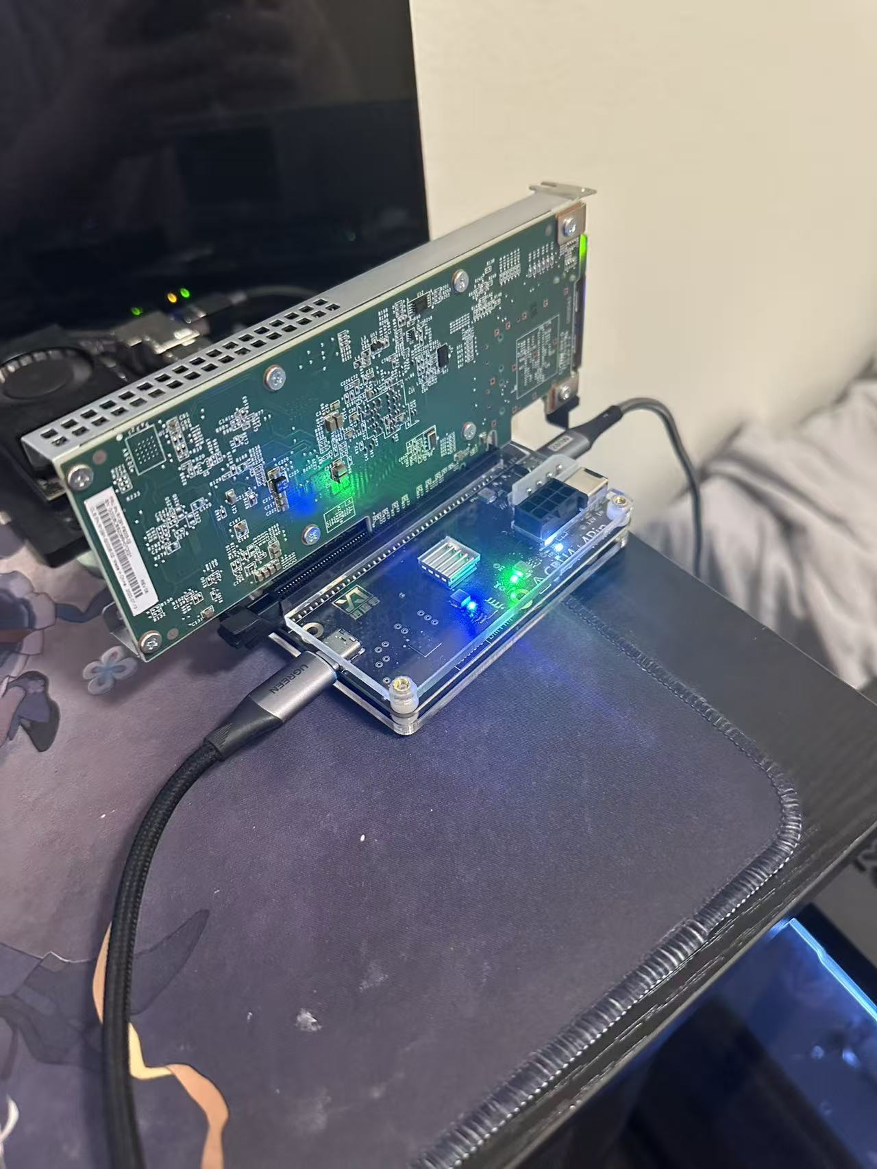
AMD/Xilinx Kintex KU3P FPGA Board
This board is my new FPGA computing platform: a Kintex UltraScale+ XCKU3P-FFVB676 accelerator card connected to my desktop through a PCIe-to-USB4 converter and powered from an external USB-PD supply. The setup lets me experiment with a serious PCIe-attached FPGA without plugging unknown second-hand accelerator hardware directly into the motherboard.
The board is closely related to the decommissioned Alibaba Cloud AS02MC04 Kintex KU3P accelerator cards documented by the FPGA reverse-engineering community. Those notes are especially useful because this class of board has strong silicon resources, high-speed I/O, and PCIe connectivity, but much less official board-level documentation than a normal development kit.
Hardware Summary
| Area | Details |
|---|---|
| FPGA | AMD/Xilinx Kintex UltraScale+ XCKU3P-FFVB676 |
| Logic | 356K system logic cells and about 163K CLB LUTs |
| DSP | 1,368 DSP slices |
| On-chip memory | 26.2 Mb total memory, including BRAM/UltraRAM resources depending on device configuration |
| High-speed I/O | 16 GTY transceivers, with the KU3P family supporting up to 32.75 Gb/s GTY links |
| Board connectivity | PCIe edge connector, two SFP+/SFP28-style cages on the Alibaba Cloud reference board family, JTAG access, and user LEDs |
| Current host setup | Desktop connection through PCIe-to-USB4 bridge plus external USB-PD power |
| Main use case | FPGA compute design, PCIe host/device experiments, and systolic-array acceleration |
AMD positions the Kintex UltraScale+ family for packet processing, data-center network acceleration, DSP-heavy workloads, and low-latency adaptable compute. For my purposes, the important part is the combination of DSP slices, on-chip memory, and PCIe/GTY connectivity: it is large enough to prototype real accelerator datapaths, but still practical enough to use as a personal lab board.
Why This Board Is Interesting
Most small FPGA boards are excellent for learning RTL, buses, and peripherals, but they quickly run out of DSPs, memory bandwidth, or high-speed I/O when the design becomes a compute accelerator. The KU3P gives me a much more realistic target for:
- Matrix multiplication and convolution-style datapaths
- Low-precision integer arithmetic, such as INT8, INT4, or packed smaller formats
- Weight-stationary and output-stationary systolic-array dataflows
- PCIe-attached DMA movement between the host and FPGA
- BRAM/URAM tiling strategies for accelerator workloads
- Hardware performance counters, backpressure behavior, and host-driver interaction
The board also has enough external connectivity to grow beyond a local PCIe lab setup. The SFP-class transceiver cages on the referenced AS02MC04 design make it interesting for future Ethernet or custom high-speed serial experiments, while PCIe is the most natural first path for desktop-hosted compute.
Desktop Connection
My current bring-up configuration uses a PCIe-to-USB4 converter and an external USB-PD power supply. This is useful for isolating power and reducing risk during early experiments, especially while I am still verifying the board state and previous flash contents.
The tradeoff is that this path is not the same as placing the card directly in a workstation PCIe slot. USB4 PCIe tunneling can add bridge-specific behavior around reset, hotplug, bandwidth negotiation, BAR mapping, and power sequencing. For early bring-up, enumeration, JTAG programming, and small DMA tests, that is acceptable. For final accelerator benchmarking, I will treat the USB4 bridge as a development convenience rather than the performance baseline.
Bring-Up Plan
1. Power and Thermal Sanity Check
The first goal is to confirm that the board powers cleanly and stays thermally controlled.
- Verify the USB-PD supply can provide the required power budget.
- Check that the external power path and adapter are stable before attaching the board to the host.
- Watch board LEDs, regulator behavior, and FPGA package temperature during idle.
- Use SYSMON through JTAG once JTAG access is available to monitor temperature and rails.
- Add active airflow before running sustained DSP-heavy workloads.
For a second-hand accelerator card, power and cooling are not boring details. They decide whether every later debug session is trustworthy.
2. PCIe Enumeration
The next step is to see what the host detects.
Useful commands:
lspci -nn
lspci -vvv -s <bus:device.function>
dmesg | rg -i "pcie|xilinx|fpga|dabc|9034"
The community notes show that these boards can appear as PCIe endpoints when the previous flash image is still present. In the Alibaba Cloud bring-up writeup, the card exposed endpoint capabilities including an x8 Gen3 link capability, even when tested through a reduced-width adapter. That is a good sign for board liveness, but it does not prove that my own future design or driver is working yet.
For my own experiments, I want to record:
- Vendor ID and device ID
- PCIe class code
- Link speed and negotiated width
- BAR sizes and address assignment
- Whether the bridge maps memory correctly through USB4
- Reset behavior after warm reboot, cold boot, and bitstream reload
3. JTAG and Bitstream Loading
JTAG is the safest path for early development because it allows temporary SRAM configuration without touching onboard flash. The reverse-engineering references describe a practical workflow using Vivado to build a design, export an SVF, and replay it through OpenOCD/J-Link. A standard AMD/Xilinx programming cable should also be a natural option if available.
My first JTAG milestones are:
- Confirm the scan chain and device ID.
- Read SYSMON temperature and voltage information.
- Load a minimal LED or counter design.
- Keep flash untouched until the board constraints and reset behavior are well understood.
- Automate bitstream generation so iteration time stays low.
This step matters because the board is powerful, but it is not a polished evaluation kit. A repeatable programming flow is the foundation for every compute experiment after it.
4. Constraints and Board-Level Mapping
Before writing any serious accelerator, I need a trusted constraints file. The public AS02MC04 notes document useful board-level clues such as the PCIe lane mapping, LED pins, reset line, and likely external clocks. The writeup identifies a 100 MHz clock pair suitable for a global clock and a 156.25 MHz reference clock likely tied to SFP use.
The careful path is:
- Start with a minimal constraints file for clock, reset, and LEDs.
- Verify simple fabric logic before enabling PCIe.
- Add PCIe constraints only after lane mapping and reference clock assumptions are checked.
- Keep transceiver and SFP experiments separate from the first compute design.
5. PCIe Data Movement
Once basic programming works, the first real system test will be a PCIe memory-mapped or DMA design. A compute accelerator is only useful if data movement is boring and measurable.
Possible starting points:
- Xilinx DMA/PCIe IP for a vendor-supported route
- LitePCIe/LiteX for an open-source SoC-style bring-up path
- A small custom BAR-mapped register block for status, control, and counters
The LiteX board-support issue for the Alibaba KU3P board is especially relevant because it tracks support work around JTAG UART, SFP Ethernet, and PCIe Gen3 lane configurations. That makes it a useful reference even if I eventually choose a more custom RTL path.
Planned Systolic-Array Work
The long-term goal is to use this board for FPGA compute design, especially a systolic-array accelerator. I want the design to be more than a classroom datapath, so I will build it in stages:
Stage 1: Small Verified Array
- Implement an 8x8 or 16x16 processing-element array.
- Start with INT8 multiply-accumulate and fixed-point accumulation.
- Compare RTL simulation outputs against a Python or NumPy golden model.
- Add per-tile start/done control and basic performance counters.
Stage 2: Local Memory and Tiling
- Add input, weight, and output buffers in BRAM or URAM.
- Support tiled matrix multiply so larger matrices can stream through a smaller PE array.
- Explore weight-stationary and output-stationary modes.
- Measure how buffer layout affects stalls and utilization.
Stage 3: PCIe Host Integration
- Move matrices from the desktop host into FPGA buffers.
- Launch kernels through a control register interface.
- Return output tiles to host memory.
- Validate correctness against CPU results across matrix sizes and quantization modes.
Stage 4: Performance Exploration
- Scale PE count until timing, routing, memory bandwidth, or PCIe transfer overhead becomes the limiting factor.
- Try INT4 or packed low-precision arithmetic.
- Add double buffering so transfer and compute can overlap.
- Instrument utilization, cycles per tile, effective GOPS/TOPS, and host-to-device overhead.
This board is a good target for that progression because the XCKU3P has enough DSPs for a meaningful MAC fabric and enough memory to make tiling experiments realistic. The most interesting engineering question will be balancing the compute array against memory organization and PCIe data movement.
Risks and Constraints
- Board documentation is community-driven, so every pinout assumption needs verification.
- PCIe-to-USB4 tunneling may limit link width, bandwidth, reset behavior, or BAR mapping.
- Power delivery and cooling must be handled externally and tested under load.
- Flash should not be overwritten until the JTAG flow and known-good bitstream are reliable.
- PCIe endpoint designs require careful host-side driver or userspace access planning.
- Timing closure on a wide systolic array may become harder than the initial RTL suggests.
Current Status
The board is physically connected to my desktop through the PCIe-to-USB4 converter and powered externally through USB-PD. The immediate next milestone is board bring-up: confirm power stability, inspect PCIe enumeration, establish JTAG access, and run a minimal test design. After that, I can move toward a small PCIe-controlled compute kernel and then a tiled systolic array.
Technical References
- AMD Kintex UltraScale+ FPGA product page - official device-family overview and KU3P resource table.
- Alibaba cloud FPGA: the 200$ Kintex UltraScale+ - detailed AS02MC04 reverse-engineering and bring-up notes covering PCIe enumeration, JTAG, OpenOCD/SVF loading, clocks, and pinout discovery.
- dkozel/Alibaba-Cloud-FPGA - collected notes for the Alibaba Cloud AS02MC04 Kintex KU3P UltraScale+ board, including board connectivity and LiteX-oriented work.
- LiteX Boards issue #705 - discussion tracking Alibaba Cloud AS02MC04 board support, including JTAG UART, SFP, and PCIe Gen3 testing goals.